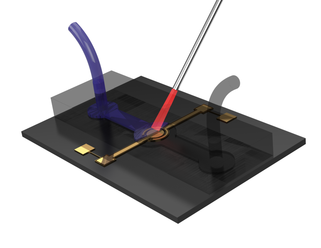
PMUT Microfluidics interface
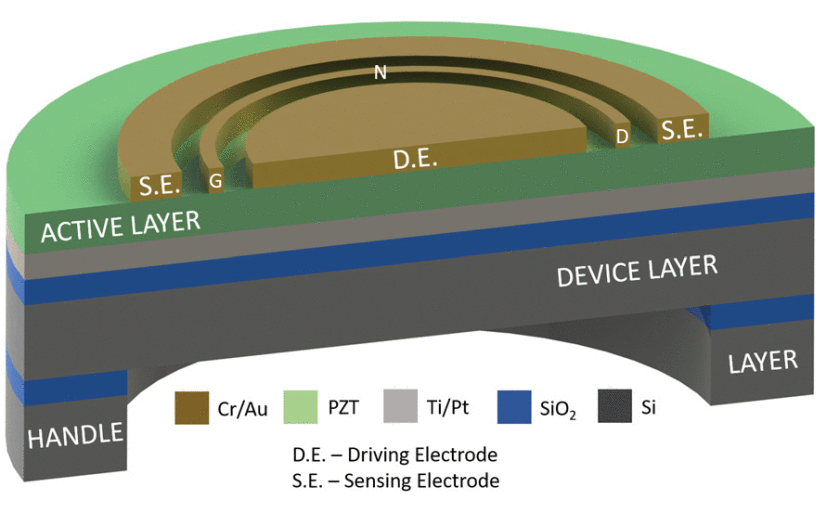
The PMUTs used in this work were fabricated at the National nanofabrication Centre, the Centre for Nano Science and Engineering, Indian Institute of Science, Bangalore. These devices use lead zirconate titanate (PZT) as the active layer. A PZT thin film of thickness ~500 nm was deposited on a platinized silicon-on-insulator (SOI) substrate having a constant device layer thickness of 10 μm. This PZT deposition was done at the National Aerospace Laboratories, Bangalore. The fabricated PMUTs incorporate two active electrodes, namely the driving electrode (D.E.) and the sensing electrode (S.E.). The fabricated PMUTs were circular in shape and could be designed to operate at desired frequencies. This is done by either varying the diameter, the thickness of the diaphragm stack, or the interlayer stresses. In this work, the diameter of the PMUTs was varied in order to obtain desired frequencies while keeping all other design variables fixed (thickness of the diaphragm was fixed at ∼10.5 μm and the interlayer residual stresses at ~700 MPa, tensile).
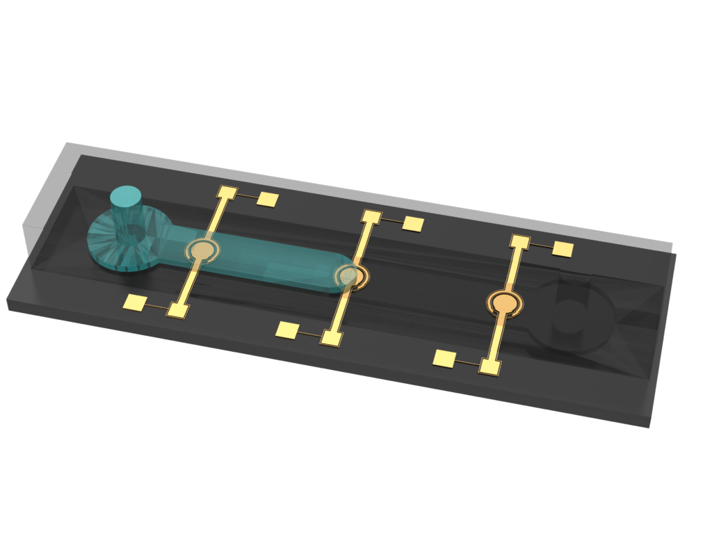
A microfluidic channel was integrated with PMUTs. This was done by fabricating a single PDMS channel having an inlet and an outlet, aligning, and bonding it to a specially designed PMUT array containing three PMUTs. For convenience, we name this device PMUT-Microfluidic-Integration (PMI). It forms a self-sensing platform to monitor fluid density in microfluidic regimes.